
Electro Static Discharge (ESD) can damage PCBs during several stages like design, assembly, testing, or field usage. ESD is a sudden flow of current between electrically charged conductors due to a difference in their voltage levels. The energy released can damage the conductive medium. A PCB coming in contact with any charged substance like assembly equipment, test probes, or even the operator may get damaged due to the ESD effect.
Static electricity is discharged within a couple of microseconds and may not be usually perceived by humans. But the damage caused to the PCBs and electronic components can be either disastrous or latent. The energy discharged can damage expensive appliances or cause a fire. In other cases, the effect may look trivial on initial inspection but might decline the circuit functionality after some time. This may even reduce the product’s lifespan.
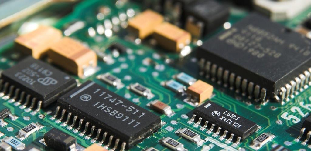
SMT assembly method is commonly used by contract manufacturers in the PCB industry. To ensure the consistent operation of the PCB product, it is necessary to avoid ESD damage during the design and assembly stages. A static charge can be developed due to friction on the SMT assembly floor. A simple human movement can build a static charge of a few thousand volts which can cause permanent damage to static-sensitive components. Assembly and test equipment can accumulate charges due to induction or by direct connection with a charged substance. This further affects PCBs when they come in contact with the assembly setup or testing devices.
Impact of ESD on PCB assembly:
The extent of ESD damage on a PCB may not be visible immediately. But it will deteriorate the board’s performance gradually. Devices like FPGAs, PLDs, etc are highly susceptible to ESD damage. The growing requirements for miniaturized products, designed for multiple functionalities depend on reliable surface mount devices (SMD).
Thin insulating layers are used in the PCB stack-up and fine traces are routed to accommodate the compact design requirements. This will affect the board’s capacity to withstand any high voltages applied. SMDs are mostly damaged in the process of storage and transportation due to ESD. Up to 30% of electronic failures are attributed to ESD damages. By strictly following the ESD preventive measures, a huge cost can be saved during the SMT assembly.
The percentage of PCB failures due to latent ESD damages is quite high compared to the instantaneous ESD damages. Components that are affected by ESD are not easily recognized but may disrupt the circuit operation. Unstable or partial functionality becomes a challenge while debugging. The extra time required for rework will add to the production cost.
There are several measures followed by PCB designers and contract manufacturers to successfully handle the ESD issues in the SMT assembly units. For guidance on static electricity safe practices and to avoid fire or explosions, you can refer to NFPA 77 standards.
Guidelines to prevent ESD damages in SMT assembly:
- In the assembly workshops, a conductive floor mat should be used in ESD-sensitive areas. This will assist in discharging any static charge built on the operator or the assembly equipment. To improve the longevity of the conductive floor mats, it is necessary to avoid any sharp object friction against the mat. Regular maintenance and cleaning of the conductive floor mat can upkeep its ability to ground the static charges effectively.
- Relative humidity can directly influence the ESD effect in the workshop. It is recommended to maintain room humidity around 40-60% at a temperature of 18-22°C. This will reduce a static charge build-up on the surfaces, as moisture in the air can act as a good conductor. It is also necessary to check if the humidity content is too high to corrode or damage any moisture-sensitive components.
- Using anti-static floor paint and static protective material in the workshop can add to the ESD protection system. It is necessary to keep the entire place free from static electricity. This includes floor, walls, doors, workstations, and manufacturing tools also.
- Technicians and other assembly staff should wear anti-static wrist straps or heel straps inside the workshop. These are cost-effective solutions and can be easily used by the staff to ensure correct grounding. Additionally, there are anti-static aprons, shoes, gloves, and caps that can be used in highly-sensitive work areas to avoid any static charge and other contaminations.
- Identify and separate the sources of static charge in the work area. Replacing regular equipment with non-static alternatives and minimizing the usage of insulating materials like paper or bubble wrap in static-sensitive areas are good ways to reduce ESD damage.
- Ensure that the assembly racks are properly grounded. Equipment carriers and other movement vehicles used to shift materials should be discharged before entering the static-sensitive areas.
- In the PCB test setups, it is recommended to use a Transient Voltage Suppressor (TVS) at the point of external connection to protect the PCB and any sensitive components mounted on it.
- PCBs should be cleaned with non-static spray during the assembly or testing process.
- In the case of insulators, ion neutralizers are used to remove any electrostatic charge build-up.
- The PCB parts and assemblies should be packed using anti-static covers, also known as ESD bags during shipment or storage.
- It is necessary to conduct regular checks on the assembly floor to evaluate if the ESD preventive measures are diligently followed. There should not be any disjointed grounding lines or loose contacts in the workshop. Conducting periodic training for the operators and other assembly staff will highlight the importance of ESD guidelines.
- Displaying the rules and warnings using sign boards in ESD-protected areas is recommended to restrict any unauthorized movements. A complete ESD protection control procedure has to be established and agreed upon by all the associated teams.
Conclusion:
ESD damages can cause a serious hazard during the PCB assembly process. It is necessary to include ESD protection in every stage of PCB development. The suggested preventive measures help electronic manufacturers to mitigate ESD damages along with reduced debugging and rework efforts while in the PCB manufacturing stage. Strictly following these guidelines can improve the lifespan and performance of PCB products.
You may also want to read,


